Polyimide Substrates, Polyimide Applications and Polyimide Properties

|
|
Unfilled Polyimide Wafers and Polyimide Substrates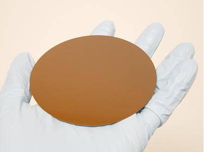
Polyimide WaferPolyimide wafers, substrates, and precise polyimide shapes are now available from Valley Design. Ultra-thin, ground, lapped or polished pure unfilled polyimide is ideal for thin films, solar cell substrates, multilayer substrates, MEMS microstructures and packaging applications.Why Polyimide?
Polyimide wafers polished on one side with 5nm Ra surface finish available from stock:
Valley Design's special polyimide processing capabilities:
Please call or email for a quotation to meet your requirements. Valley Design Corp. manufactures polished polyimide wafers under license from Opticomp Networks US Patents No. 6, 563, 998 and 6, 807, 328.
|
||||||||||||||||
|
|
Valley Design East
Phoenix Park Business Center 2 Shaker Road, Bldg. E-001 Shirley, MA 01464 Phone: 978.425.3030 Fax: 978.425.3031 Valley Design West Santa Cruz, CA 95060 Phone: 831.420.0595 Fax: 831.420.0592 


©2015 Valley Design Corp. All Rights Reserved |